TECH
India’s Semiconductor Leap: 2 nm Chips Designed from India Signal a Strategic Technological Shift

In a development being widely recognised as a milestone for India’s semiconductor ambitions, engineers based in the country have played a central role in designing 2 nanometre (nm) semiconductor chips — one of the most advanced chip technologies in existence today. This achievement, marked by a successful 2 nm chip tape-out at a leading global chipmaker’s Indian facilities, underscores a significant shift in India’s role in the global semiconductor value chain from primarily back-office support to end-to-end engineering and advanced chip design.
What Is a 2 nm Chip and Why It Matters
In semiconductor terminology, the “nanometre (nm)” designation refers to the scale of the technology node — essentially the size of the features etched onto a chip. As technology nodes shrink, chips become more power-efficient, faster and capable of packing more transistors in the same physical space. The 2 nm node represents one of the most cutting-edge levels of chip design, sitting at the forefront of global semiconductor innovation alongside 3 nm and 4 nm processes.
These advanced chips are expected to power future generations of smartphones, artificial intelligence (AI) systems, edge devices, data centre hardware, autonomous systems and high-performance computing applications. The density and complexity at this level — with tens of billions of transistors on a single die — enable significant improvements in performance and energy efficiency over earlier generations.
The India Breakthrough: Design in Bengaluru and Beyond
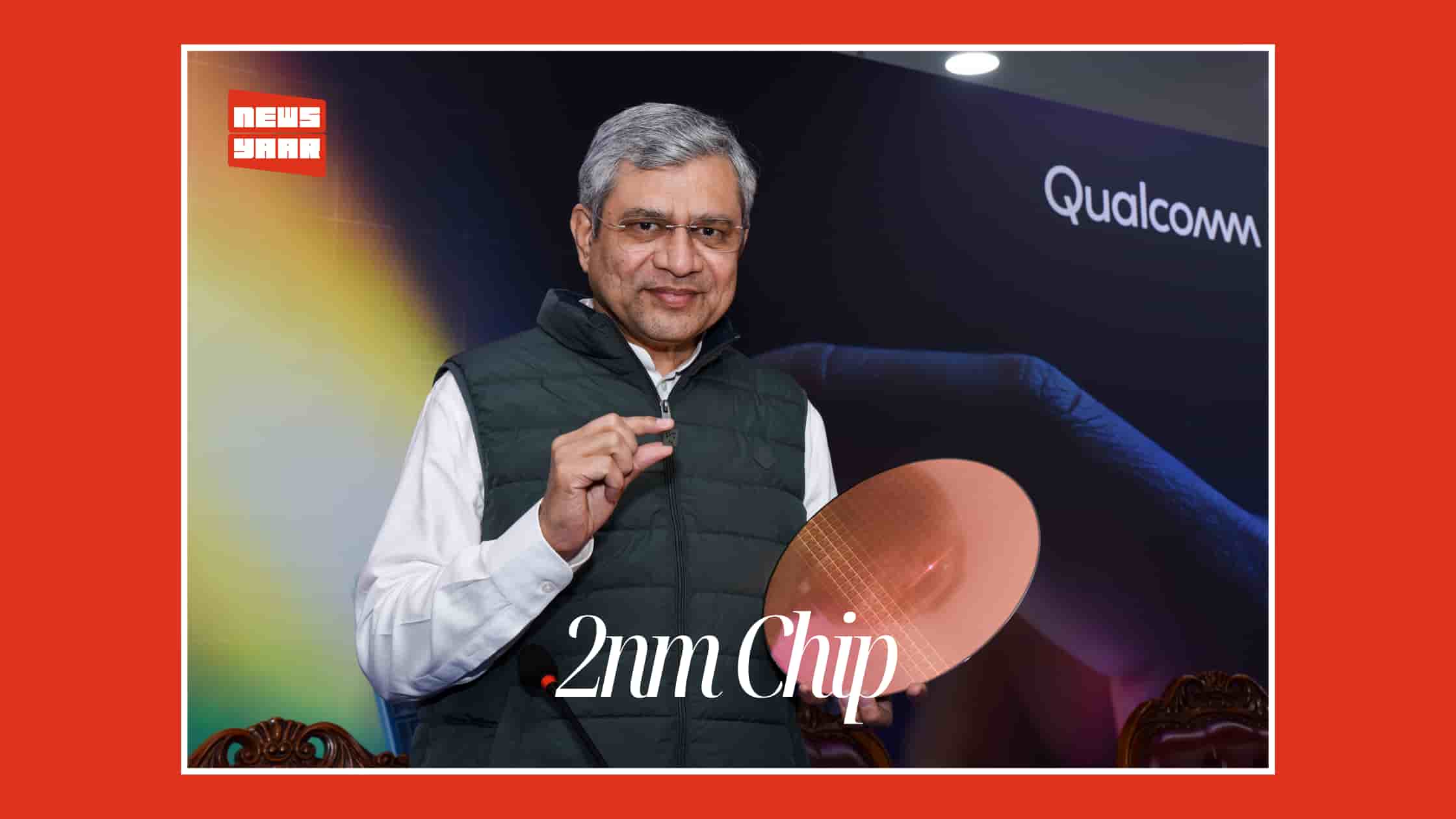
The chip design milestone was publicly showcased at **Qualcomm Technologies’ engineering centre in Bengaluru, where the company completed the **tape-out of its 2 nm semiconductor design, with development contributions distributed across its Indian engineering hubs in Bengaluru, Chennai and Hyderabad. “Tape-out” refers to the stage in chip development where the final design is completed and ready for manufacturing at a wafer fab — a critical endpoint of the design phase.
While the actual manufacturing (fabrication) of the 2 nm chips will continue to be handled by specialised semiconductor foundries overseas due to the extremely capital- and technology-intensive infrastructure required, the fact that high-end design work is being led from India reflects a meaningful advance in the country’s engineering capabilities.
Government Perspectives and Industry Interpretation
Union Minister for Electronics and Information Technology, Ashwini Vaishnaw, highlighted this development as a marker of India’s transition toward holistic semiconductor capabilities, emphasising that the country is moving beyond “back-office development work” toward complete engineering cycles — from product definition, design and silicon layout to tape-out and validation — all conducted within Indian talent pools.
At a press conference during the event, Minister Vaishnaw noted that this achievement demonstrates how India’s semiconductor design ecosystem has matured and is now integral to global engineering efforts. He indicated that the next strategic target would be to establish semiconductor “fabs” (fabrication facilities) in India, which would enable domestic production of advanced chips.
Experts emphasise that such milestones are not merely technical achievements but also symbolic markers of India’s growing integration into the global semiconductor landscape, particularly in high-end design work that drives product performance and innovation.
India as a Growing Engineering Hub
The development also puts into sharp focus India’s rapidly expanding semiconductor ecosystem — one that combines a deep talent pipeline with increasing participation from global chipmakers. India hosts one of the largest engineering workforces outside the United States for companies like Qualcomm, which have invested in design, validation, system-level optimisation and AI integration efforts for next-generation chip platforms.
Indian engineering teams contribute across multiple stages of semiconductor development, including architecture implementation, system integration and advanced feature validation — competencies that are critical in designing chips competitive at global levels.
Policy Momentum: Semicon Mission 2.0 and Indigenous Design Focus
The Government of India’s semiconductor policy framework, particularly Semicon Mission 2.0, prioritises indigenous chip design as a key objective alongside talent development, equipment and material ecosystem building, and eventual manufacturing capacity expansion. The revised mission includes funding and incentives for design-led startups, R&D centres, industry collaborations and skill development, aimed at creating a future-ready semiconductor workforce.
Under this framework, global companies setting up design operations in India — including multinational firms like Arm — reflect international confidence in Indian engineering capabilities. Such initiatives help build intellectual property (IP), research expertise and design capability at a world-class level.
Broader Strategic and Economic Implications
The design of 2 nm chips from Indian engineering centres carries significance beyond technology alone. It contributes to:
- Enhanced strategic positioning in global semiconductor supply chains
- Attraction of further foreign direct investment (FDI) in high-tech R&D
- Upskilling of engineering talent and creation of advanced tech jobs
- Foundation for future advanced manufacturing and fab development
- Integration with AI, edge computing and next-gen connectivity sectors
By enabling Indian engineers to work at the forefront of semiconductor design, the country is positioning itself as a competitor and collaborator in the high-performance chip ecosystem — a space historically dominated by a handful of global players.
Conclusion: A Step Toward a Global Semiconductor Role
While India’s semiconductor journey — from design to full-scale manufacturing — remains a multi-decade endeavour, the successful 2 nm chip tape-out driven by Indian talent and engineering operations represents a strategic inflection point. It reinforces the narrative that India is not just a consumer of cutting-edge technologies but a contributor and innovator, capable of playing a meaningful role in one of the most consequential fields of modern technology.
This milestone, achieved through collaboration between global industry leaders and Indian engineers under supportive policy frameworks, signals that the country is steadily moving up the semiconductor value chain — from design and verification to eventual productisation and broader ecosystem participation.
Video credit: YT@/ANI


