

India AI Impact Summit 2026: Detailed Agenda for Global AI Action in New Delhi
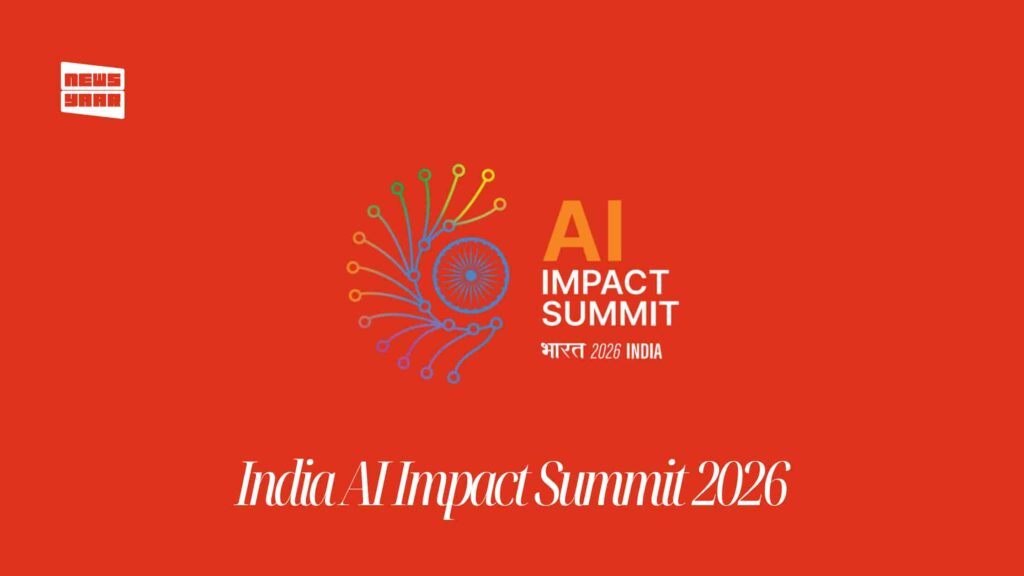
New Delhi, February 9, 2026 – India gears up for the India AI Impact Summit 2026, set for February 16-20 at Bharat Mandapam, Pragati Maidan, New Delhi, the primary venue for the India AI Impact Summit 2026, which will host the main events on February 19-20.Hosted by the Ministry of Electronics and Information Technology (MeitY), this first Global South edition, billed by Union Minister Ashwini Vaishnaw as the “largest yet,” transitions AI discourse from vision to verifiable impact under the “Three Sutras”: People, Planet, and Progress.Some sources mention a broader program across February 16-20, potentially using additional Delhi venues like Sushma Swaraj Bhawan for side events, sessions, or exhibitions. Bharat Mandapam, one of India’s largest convention centers, was upgraded by NDMC for this flagship gathering. Chief Guests and Stellar LineupPrime Minister Narendra Modi serves as the Chief Guest, inaugurating on February 16 with a keynote and hosting a leaders’ dinner. Expected heads of government include representatives from Singapore, the UAE, and Brazil (15-20 total), plus 50+ ministers. Key speakers feature Google’s Sundar Pichai, Anthropic’s Dario Amodei, Microsoft’s Satya Nadella, and Indian luminaries like Nandan Nilekani (Infosys co-founder) and Ola’s Bhavish Aggarwal. Over 40 CEOs from Reliance, TCS, and global firms join, along with a Chinese delegation, signaling a thaw in collaboration. Event Schedule and Dialogues Feb 16: Inauguration, Modi address, CEO roundtable.Feb 17-18: Plenary sessions and seven “Chakras” (working groups) on core topics.Feb 19: Startup showcase (500+ ventures), AI model launches, bilateral dialogues.Feb 20: Closing with actionable declarations.Expect 500+ parallel sessions, hackathons, and exhibitions. Dialogues include G20-style tracks on AI ethics, public-private partnerships, and Global South priorities. Participating Governments in India AI Impact Summit 2026 The summit, hosted by India’s Ministry of Electronics and Information Technology (MeitY) under the IndiaAI Mission, expects involvement from over 100 countries. Key highlights:High-Level Representation: 15-20 heads of government and 50+ ministers confirmed, including from Singapore, UAE, Brazil, and others.China: Delegation attending after India’s formal invitation, signaling AI collaboration.Preceding Hosts: Builds on summits by UK (2023 Bletchley), South Korea (2024 Seoul), France (2025 Paris).Collaborators: NITI Aayog (India’s policy think tank), state governments like Uttarakhand (pre-summit host), and international bodies (ITU, World Economic Forum).Global Engagement: Multinational working groups across Chakras, with US, UK, EU, and ASEAN nations active in prep consultations. Key Topics and Seven ChakrasThe India AI Impact Summit 2026 is structured around three foundational “Sutras” (People, Planet, Progress) that guide its discussions, with seven interconnected “Chakras” (working groups) translating these into specific, actionable themes.Core SutrasPeople: Focuses on human-centric AI, including safeguarding rights, enhancing access to services (e.g., healthcare, education), building user trust, workforce reskilling amid job impacts, and ensuring equitable benefits across societies.Planet: Addresses sustainable AI deployment, such as energy-efficient models, responsible resource use (e.g., reducing GPU/data center power demands), and AI applications for climate action, environmental monitoring, and resilience.Progress: Emphasizes inclusive innovation, capacity-building, productivity gains in sectors like agriculture and manufacturing, economic growth, and bridging the AI divide for the Global South. Seven Chakras (Key Discussion Topics)These working groups, involving 100+ countries, cover:AI governance and ethical frameworks.Trust and safety protocols for AI models (e.g., bias mitigation, transparency).AI’s impact on work and future jobs.Sector-specific applications (healthcare, agriculture, industry).Innovation and scalable solutions.Sustainability and environmental integration.Equitable access, inclusion, and development outcomes.Sessions will also spotlight IndiaAI Mission launches, startup innovations, and global standards, prioritizing “on-ground” results over regulations. What to Expect in India AI Summit?MeitY leads with partners like NITI Aayog, NASSCOM, World Economic Forum, and ITU. Corporate backers include Google, Microsoft, NVIDIA (GPU focus), and Indian firms like Tata and Adani (data centers). Governments from US, UK, EU, and ASEAN collaborate. Attendees (10,000+), policymakers, researchers, startups, NGOs, can expect networking zones, live demos (e.g., edge AI), policy labs, and a “Global AI Talent Fair.” Launches include indigenous foundational models under the Rs 10,370 crore IndiaAI Mission. India’s Strategic Push Amid HurdlesEchoing Bletchley (2023), Seoul (2024), and Paris (2025), India’s summit prioritizes “on-ground” wins for 1.4 billion people, as per Secretary S. Krishnan. AI could add $500B to GDP (NASSCOM), but challenges like GPU imports persist—eased by US trade deals and data center tax holidays to 2047. Budget 2026-27 tweaks fund nuclear-powered AI infra, as Vaishnaw eyes energy self-reliance.Vaishnaw hailed “phenomenal” global buy-in, with NDMC upgrading venues. Beyond talks, expect MoUs on compute sharing, talent visas, and sustainable AI pacts, positioning India as an AI diplomacy hub.This summit promises not just dialogue, but deliverables: inclusive, green AI for humanity’s progress.Video credit: YT@/Digital India
DRDO’s GaN Chip Breakthrough: A Strategic Leap in India’s Defence Technology
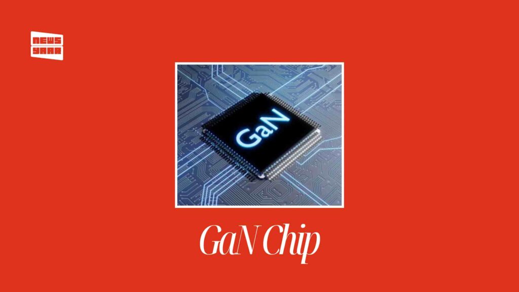
India’s Defence Research and Development Organisation (DRDO) has achieved a transformative milestone in defence electronics with the successful development of indigenous Gallium Nitride (GaN) semiconductor chips — a feat that marks a decisive shift in the country’s technological autonomy and strategic capability. This achievement, emerging from years of sustained research and innovation, places India alongside a select group of countries with advanced compound semiconductor capabilities and strengthens its defence industrial base amid evolving global security dynamics.What Are GaN Chips and Why They MatterGallium Nitride (GaN) chips represent a class of compound semiconductors that outperform traditional silicon-based technologies in power efficiency, thermal tolerance and high-frequency performance. Unlike silicon, GaN can operate at much higher power densities and elevated temperatures, making it ideal for defence systems where reliability under extreme conditions is critical. These characteristics are especially valuable in active electronically scanned array (AESA) radars, missile seekers, electronic warfare systems, communication arrays and surveillance sensors, which demand compact, high-power, high-frequency performance.Experts characterise compound semiconductor technologies like GaN and Silicon Carbide (SiC) as “thoroughbred racehorses” of modern defence electronics — systems that deliver superior range, resolution and signal fidelity in comparison with legacy counterparts.From Technology Denial to Indigenous MasteryThe journey toward GaN mastery in India began as a response to foreign technology denial regimes that restricted access to high-end semiconductor technologies during sensitive defence procurements. A notable example occurred during negotiations for the Rafale fighter jet acquisition, when France declined to transfer restricted chip-level technologies under offset requirements. Rather than accept continued dependence, Indian scientists initiated a long-term indigenous development effort led by DRDO labs.Two principal research centres spearheaded this effort:Solid State Physics Laboratory (SSPL), Delhi — focusing on material growth, device physics and compound semiconductor device design.Gallium Arsenide Enabling Technology Centre (GAETEC), Hyderabad — concentrating on compound chip fabrication, testing and integration.By late 2025 and into 2026, DRDO scientists had successfully decoded and implemented GaN technology at the level of monolithic microwave integrated circuits (MMICs) and high-power GaN High Electron Mobility Transistors (HEMTs), a critical achievement for defence electronic systems.Strategic and Operational ImplicationsThe GaN breakthrough is not merely a laboratory milestone — it has direct implications for India’s defence preparedness, sensor infrastructure and future combat platforms:Enhanced Radar and AESA Systems: GaN-based radar modules allow systems to transmit and receive much higher power with reduced heat loss, improving detection range, resolution and reliability — vital for surveillance and targeting.Missile Seekers and Electronic Warfare: GaN chips’ high-frequency handling and thermal tolerance make them suitable for compact, resilient radar seekers and EW systems used in both air-to-air and surface-to-air engagements.Communication and Satellite Systems: GaN’s superior power efficiency enhances satellite payloads and communication terminals, especially where size, weight and power constraints are critical.The integration of GaN in defence electronics also supports self-reliance in mission-critical technology, reducing dependency on imports and external suppliers. DRDO leadership has emphasised this capability as a strategic buffer against supply disruptions and export control regimes in times of geopolitical tension.Broader Technological ContextGaN development is part of a broader global emphasis on third-generation semiconductor technologies, which include GaN and SiC. These technologies are rapidly shaping defence, telecommunications, electric vehicles, power electronics and 5G infrastructure due to their ability to handle extreme operating conditions and high efficiencies.India’s achievement places it in an elite cohort of nations — including the United States, France, Russia, Germany, South Korea and China — actively pursuing sovereign GaN semiconductor capabilities.Expert Perspectives and Domestic Innovation EcosystemOfficials within DRDO, including Suma Varughese — Director General of Micro Electronic Devices and Computational Systems — have highlighted that GaN chips are not incremental advancements but foundational enablers for next-generation defence systems. These chips allow systems such as AESA radars to deliver significantly greater range and resolution, while electronic warfare setups benefit from enhanced power management and frequency agility.The GaN initiative also bolsters India’s indigenous semiconductor ecosystem, encouraging domestic research institutions, startups and industry partners to participate in high-end chip design and fabrication research.Integration into Defence PlatformsWhile the GaN chips themselves are an achievement, the ongoing work involves incorporating them into operational systems. DRDO’s progress in GaN technology aligns with advancements in long-range radars, missile guidance systems and next-generation avionics, where compound semiconductors enable performance far beyond what silicon technology can offer.Indigenous GaN technology is expected to play a key role in future sensor suites for platforms such as radar networks and upgraded fighter aircraft systems, enhancing India’s air domain awareness and electronic warfare capabilities.Strategic Autonomy and Future ProspectsFrom a strategic standpoint, achieving GaN chip capability is a milestone in India’s pursuit of technological sovereignty. DRDO’s advancements underscore a wider national effort toward self-reliance in defence technology, consistent with the government’s “Aatmanirbhar Bharat” (self-reliant India) vision.Officials estimate that mastering and iterating next-generation semiconductor technologies — including further refinement of GaN and related systems — will be a multi-year endeavour. However, the successful development of indigenous GaN chips demonstrates India’s capacity to innovate at the highest technical levels, insulating its defence industry from external constraint and positioning it for leadership in future electronic warfare technologies.Why This Breakthrough MattersThe indigenous GaN chip triumph represents more than a single technical achievement; it embodies a shift in India’s defence technology trajectory — from dependence on foreign suppliers to authentic self-sufficiency in core electronic systems. As warfare becomes increasingly reliant on advanced sensors, radar systems and digital electronics, the mastery of GaN technology equips India with tools essential for next-generation defence capabilities, operational autonomy and strategic deterrence in the evolving security environment.
India’s Semiconductor Leap: 2 nm Chips Designed from India Signal a Strategic Technological Shift
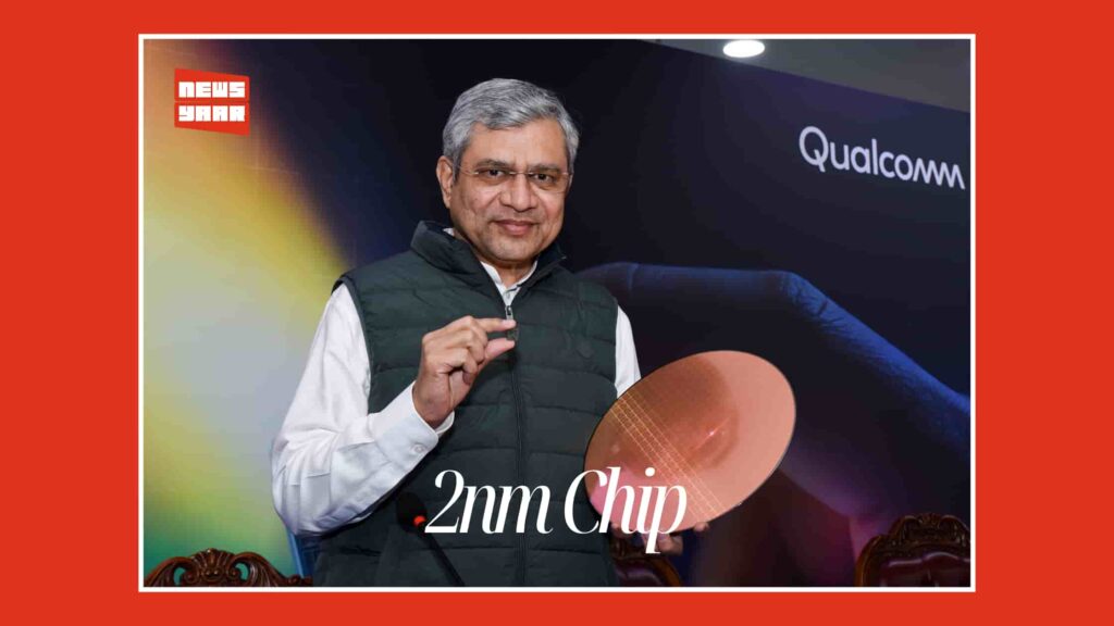
In a development being widely recognised as a milestone for India’s semiconductor ambitions, engineers based in the country have played a central role in designing 2 nanometre (nm) semiconductor chips — one of the most advanced chip technologies in existence today. This achievement, marked by a successful 2 nm chip tape-out at a leading global chipmaker’s Indian facilities, underscores a significant shift in India’s role in the global semiconductor value chain from primarily back-office support to end-to-end engineering and advanced chip design.What Is a 2 nm Chip and Why It MattersIn semiconductor terminology, the “nanometre (nm)” designation refers to the scale of the technology node — essentially the size of the features etched onto a chip. As technology nodes shrink, chips become more power-efficient, faster and capable of packing more transistors in the same physical space. The 2 nm node represents one of the most cutting-edge levels of chip design, sitting at the forefront of global semiconductor innovation alongside 3 nm and 4 nm processes.These advanced chips are expected to power future generations of smartphones, artificial intelligence (AI) systems, edge devices, data centre hardware, autonomous systems and high-performance computing applications. The density and complexity at this level — with tens of billions of transistors on a single die — enable significant improvements in performance and energy efficiency over earlier generations.The India Breakthrough: Design in Bengaluru and BeyondThe chip design milestone was publicly showcased at **Qualcomm Technologies’ engineering centre in Bengaluru, where the company completed the **tape-out of its 2 nm semiconductor design, with development contributions distributed across its Indian engineering hubs in Bengaluru, Chennai and Hyderabad. “Tape-out” refers to the stage in chip development where the final design is completed and ready for manufacturing at a wafer fab — a critical endpoint of the design phase.While the actual manufacturing (fabrication) of the 2 nm chips will continue to be handled by specialised semiconductor foundries overseas due to the extremely capital- and technology-intensive infrastructure required, the fact that high-end design work is being led from India reflects a meaningful advance in the country’s engineering capabilities.Government Perspectives and Industry InterpretationUnion Minister for Electronics and Information Technology, Ashwini Vaishnaw, highlighted this development as a marker of India’s transition toward holistic semiconductor capabilities, emphasising that the country is moving beyond “back-office development work” toward complete engineering cycles — from product definition, design and silicon layout to tape-out and validation — all conducted within Indian talent pools.At a press conference during the event, Minister Vaishnaw noted that this achievement demonstrates how India’s semiconductor design ecosystem has matured and is now integral to global engineering efforts. He indicated that the next strategic target would be to establish semiconductor “fabs” (fabrication facilities) in India, which would enable domestic production of advanced chips.Experts emphasise that such milestones are not merely technical achievements but also symbolic markers of India’s growing integration into the global semiconductor landscape, particularly in high-end design work that drives product performance and innovation.India as a Growing Engineering HubThe development also puts into sharp focus India’s rapidly expanding semiconductor ecosystem — one that combines a deep talent pipeline with increasing participation from global chipmakers. India hosts one of the largest engineering workforces outside the United States for companies like Qualcomm, which have invested in design, validation, system-level optimisation and AI integration efforts for next-generation chip platforms.Indian engineering teams contribute across multiple stages of semiconductor development, including architecture implementation, system integration and advanced feature validation — competencies that are critical in designing chips competitive at global levels.Policy Momentum: Semicon Mission 2.0 and Indigenous Design FocusThe Government of India’s semiconductor policy framework, particularly Semicon Mission 2.0, prioritises indigenous chip design as a key objective alongside talent development, equipment and material ecosystem building, and eventual manufacturing capacity expansion. The revised mission includes funding and incentives for design-led startups, R&D centres, industry collaborations and skill development, aimed at creating a future-ready semiconductor workforce.Under this framework, global companies setting up design operations in India — including multinational firms like Arm — reflect international confidence in Indian engineering capabilities. Such initiatives help build intellectual property (IP), research expertise and design capability at a world-class level.Broader Strategic and Economic ImplicationsThe design of 2 nm chips from Indian engineering centres carries significance beyond technology alone. It contributes to:Enhanced strategic positioning in global semiconductor supply chainsAttraction of further foreign direct investment (FDI) in high-tech R&DUpskilling of engineering talent and creation of advanced tech jobsFoundation for future advanced manufacturing and fab developmentIntegration with AI, edge computing and next-gen connectivity sectorsBy enabling Indian engineers to work at the forefront of semiconductor design, the country is positioning itself as a competitor and collaborator in the high-performance chip ecosystem — a space historically dominated by a handful of global players.Conclusion: A Step Toward a Global Semiconductor RoleWhile India’s semiconductor journey — from design to full-scale manufacturing — remains a multi-decade endeavour, the successful 2 nm chip tape-out driven by Indian talent and engineering operations represents a strategic inflection point. It reinforces the narrative that India is not just a consumer of cutting-edge technologies but a contributor and innovator, capable of playing a meaningful role in one of the most consequential fields of modern technology.This milestone, achieved through collaboration between global industry leaders and Indian engineers under supportive policy frameworks, signals that the country is steadily moving up the semiconductor value chain — from design and verification to eventual productisation and broader ecosystem participation.Video credit: YT@/ANI
Indian Startups at CES 2026: Homegrown Innovation Takes Global Spotlight in Las Vegas

Indian startups and technology firms significantly expanded their presence at CES 2026 — the world’s largest technology showcase held in Las Vegas from January 6 to 9, 2026 — reflecting the country’s evolving tech ambitions and increasing global competitiveness. The annual event, organised by the Consumer Technology Association (CTA), attracted more than 4,100 exhibitors from around 150 countries, underscoring its role as a launchpad for next-generation innovations spanning artificial intelligence (AI), digital health, robotics, mobility, enterprise technology and immersive entertainment.According to CTA executives, Indian participation has steadily grown, with a broader range of startups and established firms using the platform to showcase their products, engage with global partners and position themselves for international expansion. Indian delegations this year included innovators from healthtech, wearables, robotics and automotive systems, signalling the ecosystem’s transition from domestic focus to global impact.Ultrahuman: Metabolic Health and WearablesOne of the headline Indian participants at CES 2026 was Ultrahuman, a Bengaluru-based health technology firm co-founded by Mohit Kumar, Vinay Bhargava and Vatsal Singhal. The company displayed its suite of wearable health devices and preventive care platforms, including what it bills as the world’s lightest sleep-tracking wearable, a continuous glucose monitoring (CGM) system and a preventive blood testing solution designed to empower users with metabolic insights. Ultrahuman’s presence marked India’s growing footprint in consumer health tech at global forums.Noise: Smart Wearables Designed for Global MarketsNoise, headquartered in Gurugram and led by founders Amit Khatri and Gaurav Khatri, was another major Indian exhibitor. The company, recognised as one of the third-largest smartwatch brands in the world, showcased its latest wearable technologies at CES, emphasising advanced health metrics, design innovation and global compatibility. Noise’s participation highlighted India’s emergence not only as a producer of affordable wearables but as a designer and manufacturer capable of competing with established global brands.“We are proud to come here and compete on a world stage,” said Hamish Patel, Vice President – Product Devices at Noise, noting that the company’s R&D and manufacturing are largely based in India, enabling it to present products that match global benchmarks.aabo: MedTech InnovationsAmong the Indian startups at CES 2026 was aabo, a MedTech firm focused on AI-driven health solutions. Although not a household name, its technology emphasises the intersection of machine intelligence and healthcare delivery, an area of rising relevance as global health systems integrate data-led diagnostics and monitoring. The specifics of aabo’s product suite were highlighted among Indian exhibitors but details on founders and product characteristics are linked to its positioning as a healthtech innovator on the CES show floor.ArvyaX Technologies: Robotics and Pseudo-RealityArvyaX Technologies, founded by Shalabh Bhatnagar, showcased its robotics and pseudo-reality solutions at CES’s Eureka Park — an innovation zone dedicated to emerging startups. The Bhopal-based firm has developed technologies that blend digital and physical environments, targeting enterprise sectors such as industrial training, simulation and collaborative experiences. Shalabh Bhatnagar described participating at CES as a moment of pride, emphasising that ArvyaX’s innovations were both made and innovated in India, reflecting the nation’s rising capabilities in robotics and immersive technologies.Sona Comstar: Automotive Technology and EV SystemsThe automotive technology company Sona Comstar was another Indian participant at CES 2026, presenting its advanced electric vehicle (EV) components and systems. With a strong focus on R&D in high-power density EV motors, differential assemblies and lightweight drivetrain systems, Sona Comstar’s technology underscores India’s potential in automotive core technology development and global mobility solutions. The company’s products cater to modern EV performance requirements and highlight a broader shift toward electrification and smart mobility.Zoondia and Industry CollaborationsIn addition to standalone startups, Indian participation included Zoondia, a global technology partner offering enterprise solutions and services. Though not a startup in the strictest sense, Zoondia’s presence further reflects the breadth of Indian engagement at CES, spanning early-stage innovation to established tech services with global delivery capabilities.The Significance of Indian ParticipationExecutives at CES 2026 noted that India’s presence was broader and deeper than in previous years, building on momentum from the first dedicated Indian pavilion introduced on the CES show floor in 2024. This year’s participation spanned startups, industry bodies such as the CMAI Association of India, and firms showcasing products that compete with global innovations rather than just representing emerging market offerings.Industry observers have highlighted several key implications of India’s growing CES footprint:Global Visibility: Participation at CES elevates Indian startups to international buyers, investors and collaborators, helping them secure partnerships, pilot projects and market entry opportunities.Innovation Credibility: Demonstrating products at a major global venue signals maturity and readiness to compete on performance and design quality.Ecosystem Confidence: The increasing number of Indian participants reflects confidence among founders and investors in showcasing innovations on a global stage.Cross-Sector Representation: Startups at CES 2026 represented health tech, wearables, robotics and automotive systems, indicating that India’s startup ecosystem is diversifying beyond software into deep tech and hardware innovation.What This Means for India’s Startup EcosystemThe rising participation of Indian startups at CES 2026 comes at a time when the country’s broader startup ecosystem is experiencing structural shifts. India is now recognised as one of the largest startup ecosystems globally, with a growing emphasis on deep tech, AI, robotics and hardware innovation rather than only digital services. Initiatives such as startup support missions, increased R&D investment and industry collaborations are catalysing this transformation, enabling more Indian founders to engage in global innovation discourse and market expansion.Indian founders and CEOs attending CES emphasised that events like CES are not merely showcases but strategic platforms for networking, validation, investment engagement and collaboration, helping elevate India’s technology brands to global audiences and potential customers.Looking ForwardAs CES continues to be a global stage for breakthrough technologies, the increasing presence of Indian startups at CES 2026 reflects a broader narrative of India’s evolution from a predominantly software and services economy to a hardware and deep-tech innovator on the world stage. With continued participation in global technology showcases, Indian founders aim to build enduring technology brands that are recognised not only domestically but across markets in North America, Europe and Asia.The momentum generated at CES 2026 is expected
India’s DHRUV64: The First 1 GHz, 64-Bit Dual-Core Microprocessor
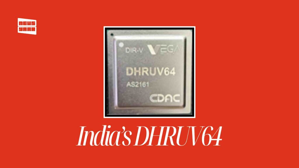
In a landmark moment for India’s semiconductor ambitions, the Centre for Development of Advanced Computing (C-DAC) has unveiled DHRUV64, the country’s first 1 GHz, 64-bit dual-core microprocessor.Developed under the government’s Microprocessor Development Programme and showcased as part of the Digital India RISC-V (DIR-V) initiative, DHRUV64 represents a major stride toward self-reliance in advanced chip design and computing technology. A Milestone in Indigenous Chip DesignDHRUV64 is built on an open-source RISC-V architecture, an increasingly popular set of instructions that allows chip designers to innovate without costly licensing fees from foreign companies.Operating at a clock speed of 1.0 GHz with dual processing cores and 64-bit capability, it brings India into the realm of gigahertz-class embedded processors, a class previously dominated by global players.Unlike earlier academic or specialised chips, DHRUV64 is designed for broader strategic and commercial applications, including industrial automation, automotive electronics, 5G infrastructure, consumer devices, and Internet of Things (IoT) systems. It supports modern operating systems, integrates with diverse hardware systems, and provides multitasking efficiency suited for a range of real-world deployments. How Does It Matter?India currently consumes roughly 20 percent of the world’s microprocessors, yet historically has relied heavily on imports for core computing technology.Developing a homegrown processor like DHRUV64 is significant not only for technological sovereignty but also for enhancing security, reducing supply-chain vulnerabilities, and building local expertise in semiconductor design.By creating a platform that domestic startups, researchers, and established companies can build upon, DHRUV64 is expected to boost innovation across the electronics ecosystem and support cheaper prototyping and product development.It also provides a foundation for a growing pipeline of skilled chip design professionals, further energising India’s tech sector.A Step Toward Aatmanirbhar Bharat in TechnologyDHRUV64 marks a continuation of India’s journey toward an Aatmanirbhar (self-reliant) semiconductor ecosystem. The chip follows earlier indigenous designs such as SHAKTI, AJIT, VIKRAM, and THEJAS64, and sits alongside future variants like Dhanush and Dhanush+ in the development pipeline.While India still relies on global fabrication technologies for manufacturing, the design and strategic deployment of processors like DHRUV64 signal a slow but steady shift toward autonomous capabilities in core computing technologies, a critical competitiveness marker in the global tech landscape.
Sanchar Saathi App: How India Is Empowering Citizens Against Telecom Fraud

Understanding the Sanchar Saathi InitiativeSanchar Saathi is a government-backed digital initiative aimed at protecting telecom users from fraud, identity theft, and the misuse of mobile connections. The app aims to bring transparency and control directly into the hands of citizens.Why the App Was Needed?India has witnessed a sharp rise in cyber fraud, fake SIM usage, and unauthorised mobile connections. Many users were unaware of the number of numbers issued in their name, making them vulnerable to misuse.Key Features Explained SimplyThe Sanchar Saathi app allows users to check mobile connections linked to their Aadhaar, block lost or stolen phones, and report suspected fraud. These features reduce dependency on telecom offices and speed up action.How It Helps Ordinary UsersFor common citizens, the app provides peace of mind. Users can instantly identify unknown connections, prevent misuse, and take quick corrective steps without technical knowledge.The launch of Sanchar Saathi reflects the government’s broader focus on digital safety and citizen empowerment. It aligns with initiatives aimed at securing India’s rapidly expanding digital ecosystem.Final WordsAs awareness grows, Sanchar Saathi could become a key tool in fighting telecom fraud nationwide. Experts believe regular updates and public education will determine its long-term success.