

PM Modi Inaugurates Micron’s Semiconductor ATMP Facility in Sanand
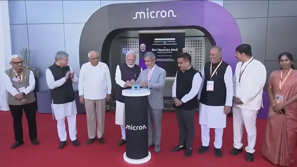
Prime Minister Narendra Modi inaugurated Micron Technology’s state-of-the-art Semiconductor Assembly, Test, and Packaging (ATMP) facility in Sanand, Gujarat, on February 28, 2026, marking India’s entry into commercial semiconductor production. This $2.75 billion milestone, the first of its kind in the country, converts advanced DRAM and NAND wafers into finished memory products for AI, data centers, and mobiles, positioning India as a key player in the global chip value chain.From MoU to Production: Lightning-Fast ExecutionThe project’s speed exemplifies India’s “New India” mindset. Signed in June 2023, groundbreaking occurred in September 2023, pilot machines installed by February 2024, and commercial production began in February 2026, just 33 months end-to-end. PM Modi highlighted streamlined regulations, like Advanced Pricing Agreements (APAs) cleared in months versus 3-5 years elsewhere, crediting clear intent and nation-first dedication.The Sanand plant boasts over 500,000 sq ft of cleanroom, one of the world’s largest single-floor ATMP cleanrooms, ISO 9001:2015 certified, LEED Gold-bound, and zero-liquid discharge via water-saving tech. First made-in-India memory modules shipped to Dell for local laptops, with tens of millions of chips expected in 2026, scaling to hundreds of millions in 2027.Micron CEO Sanjay Mehrotra, at the event with Gujarat CM Bhupendra Patel, Union Minister Ashwini Vaishnaw, and US Ambassador Sergio Gor, called it a “proud moment” building resilient AI ecosystems. Vaishnaw termed it “historic,” shifting India from chip consumer to manufacturing hub under PM Modi’s leadership.Microchips: The Oil of the 21st CenturyPM Modi framed semiconductors as the bridge from the Industrial Revolution to the AI era: “If oil regulated the last century, microchips will regulate this one.” Launched amid COVID chaos via the Semiconductor Mission, early seeds now yield fruit. India approved 10 projects under Semicon India; three more ramp up soon in Uttar Pradesh, Assam, Odisha, and Punjab, creating a pan-India ecosystem beyond factories, encompassing machines, design, R&D, logistics, and skills.Budget 2026’s India Semiconductor Mission 2.0 targets the full value chain, spurring domestic demand for materials amid booming gadget adoption. Electronics production and exports surged manifold in 11 years; “Make in India” now powers automobiles, mobiles, and tech.Sanand mirrors its auto-hub transformation, now anchoring semiconductors alongside chemicals, petrochemicals, and skill centers. Gujarat’s policies on approvals, land, and utilities boost investor faith; Dholera and Sanand emerge as Western India’s chip clusters.India-US Partnership Powers Global Supply ResilienceThe facility underscores deepening India-US ties in AI and chips, including the Pax Silica agreement from the recent AI Summit for critical minerals. The two largest democracies secure supply chains amid geopolitical flux. PM Modi messaged investors: “India is ready, reliable, delivers, capable, competitive, committed.”Micron’s Gujarat push builds talent via PDEU, Namtech, nationwide universities, and govt skills programs, focusing on STEM, advanced manufacturing, digital/AI literacy. Sustainability integrates health, safety, and eco-commitments.Broader Semiconductor Ecosystem BoomThis ATMP unit complements fabs like Tata’s in Dholera and others, addressing AI-driven memory demand. India’s electronics journey, from IT services to hardware, accelerates Viksit Bharat. Key Project MetricsDetailsKey Project MetricsDetailsInvestment$2.75B (Micron + govt)Cleanroom Size500,000+ sq ft (world’s largest single-floor ATMP)Output 2026Tens of millions of chipsOutput 2027Hundreds of millionsTimelineMoU Jun’23 → Production Feb’26States InvolvedGujarat, UP, Assam, Odisha, PunjabGlobal PartnersUS (Micron, Dell), via Pax SilicaA Tech Leadership LeapFrom software superpower to hardware contender, the nation builds self-reliant ecosystems fueling AI, mobiles, EVs. As PM Modi envisioned post-AI Summit, this hardware milestone cements technology leadership, inviting the world to co-create in a reliable, scalable hub.
India’s Semiconductor Leap: 2 nm Chips Designed from India Signal a Strategic Technological Shift

In a development being widely recognised as a milestone for India’s semiconductor ambitions, engineers based in the country have played a central role in designing 2 nanometre (nm) semiconductor chips — one of the most advanced chip technologies in existence today. This achievement, marked by a successful 2 nm chip tape-out at a leading global chipmaker’s Indian facilities, underscores a significant shift in India’s role in the global semiconductor value chain from primarily back-office support to end-to-end engineering and advanced chip design.What Is a 2 nm Chip and Why It MattersIn semiconductor terminology, the “nanometre (nm)” designation refers to the scale of the technology node — essentially the size of the features etched onto a chip. As technology nodes shrink, chips become more power-efficient, faster and capable of packing more transistors in the same physical space. The 2 nm node represents one of the most cutting-edge levels of chip design, sitting at the forefront of global semiconductor innovation alongside 3 nm and 4 nm processes.These advanced chips are expected to power future generations of smartphones, artificial intelligence (AI) systems, edge devices, data centre hardware, autonomous systems and high-performance computing applications. The density and complexity at this level — with tens of billions of transistors on a single die — enable significant improvements in performance and energy efficiency over earlier generations.The India Breakthrough: Design in Bengaluru and BeyondThe chip design milestone was publicly showcased at **Qualcomm Technologies’ engineering centre in Bengaluru, where the company completed the **tape-out of its 2 nm semiconductor design, with development contributions distributed across its Indian engineering hubs in Bengaluru, Chennai and Hyderabad. “Tape-out” refers to the stage in chip development where the final design is completed and ready for manufacturing at a wafer fab — a critical endpoint of the design phase.While the actual manufacturing (fabrication) of the 2 nm chips will continue to be handled by specialised semiconductor foundries overseas due to the extremely capital- and technology-intensive infrastructure required, the fact that high-end design work is being led from India reflects a meaningful advance in the country’s engineering capabilities.Government Perspectives and Industry InterpretationUnion Minister for Electronics and Information Technology, Ashwini Vaishnaw, highlighted this development as a marker of India’s transition toward holistic semiconductor capabilities, emphasising that the country is moving beyond “back-office development work” toward complete engineering cycles — from product definition, design and silicon layout to tape-out and validation — all conducted within Indian talent pools.At a press conference during the event, Minister Vaishnaw noted that this achievement demonstrates how India’s semiconductor design ecosystem has matured and is now integral to global engineering efforts. He indicated that the next strategic target would be to establish semiconductor “fabs” (fabrication facilities) in India, which would enable domestic production of advanced chips.Experts emphasise that such milestones are not merely technical achievements but also symbolic markers of India’s growing integration into the global semiconductor landscape, particularly in high-end design work that drives product performance and innovation.India as a Growing Engineering HubThe development also puts into sharp focus India’s rapidly expanding semiconductor ecosystem — one that combines a deep talent pipeline with increasing participation from global chipmakers. India hosts one of the largest engineering workforces outside the United States for companies like Qualcomm, which have invested in design, validation, system-level optimisation and AI integration efforts for next-generation chip platforms.Indian engineering teams contribute across multiple stages of semiconductor development, including architecture implementation, system integration and advanced feature validation — competencies that are critical in designing chips competitive at global levels.Policy Momentum: Semicon Mission 2.0 and Indigenous Design FocusThe Government of India’s semiconductor policy framework, particularly Semicon Mission 2.0, prioritises indigenous chip design as a key objective alongside talent development, equipment and material ecosystem building, and eventual manufacturing capacity expansion. The revised mission includes funding and incentives for design-led startups, R&D centres, industry collaborations and skill development, aimed at creating a future-ready semiconductor workforce.Under this framework, global companies setting up design operations in India — including multinational firms like Arm — reflect international confidence in Indian engineering capabilities. Such initiatives help build intellectual property (IP), research expertise and design capability at a world-class level.Broader Strategic and Economic ImplicationsThe design of 2 nm chips from Indian engineering centres carries significance beyond technology alone. It contributes to:Enhanced strategic positioning in global semiconductor supply chainsAttraction of further foreign direct investment (FDI) in high-tech R&DUpskilling of engineering talent and creation of advanced tech jobsFoundation for future advanced manufacturing and fab developmentIntegration with AI, edge computing and next-gen connectivity sectorsBy enabling Indian engineers to work at the forefront of semiconductor design, the country is positioning itself as a competitor and collaborator in the high-performance chip ecosystem — a space historically dominated by a handful of global players.Conclusion: A Step Toward a Global Semiconductor RoleWhile India’s semiconductor journey — from design to full-scale manufacturing — remains a multi-decade endeavour, the successful 2 nm chip tape-out driven by Indian talent and engineering operations represents a strategic inflection point. It reinforces the narrative that India is not just a consumer of cutting-edge technologies but a contributor and innovator, capable of playing a meaningful role in one of the most consequential fields of modern technology.This milestone, achieved through collaboration between global industry leaders and Indian engineers under supportive policy frameworks, signals that the country is steadily moving up the semiconductor value chain — from design and verification to eventual productisation and broader ecosystem participation.Video credit: YT@/ANI