


India’s Semiconductor Leap: 2 nm Chips Designed from India Signal a Strategic Technological Shift
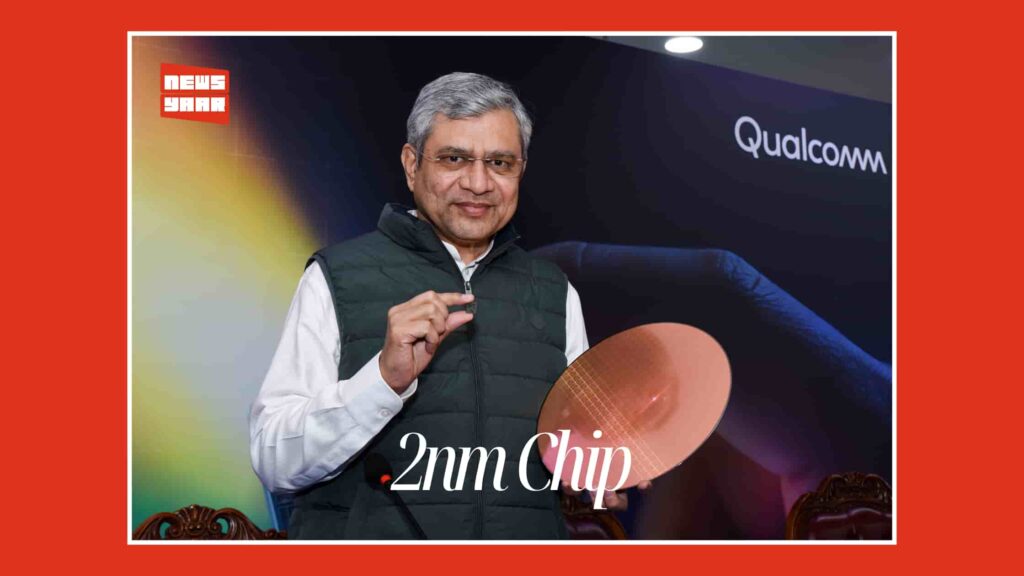
In a development being widely recognised as a milestone for India’s semiconductor ambitions, engineers based in the country have played a central role in designing 2 nanometre (nm) semiconductor chips — one of the most advanced chip technologies in existence today. This achievement, marked by a successful 2 nm chip tape-out at a leading global chipmaker’s Indian facilities, underscores a significant shift in India’s role in the global semiconductor value chain from primarily back-office support to end-to-end engineering and advanced chip design.What Is a 2 nm Chip and Why It MattersIn semiconductor terminology, the “nanometre (nm)” designation refers to the scale of the technology node — essentially the size of the features etched onto a chip. As technology nodes shrink, chips become more power-efficient, faster and capable of packing more transistors in the same physical space. The 2 nm node represents one of the most cutting-edge levels of chip design, sitting at the forefront of global semiconductor innovation alongside 3 nm and 4 nm processes.These advanced chips are expected to power future generations of smartphones, artificial intelligence (AI) systems, edge devices, data centre hardware, autonomous systems and high-performance computing applications. The density and complexity at this level — with tens of billions of transistors on a single die — enable significant improvements in performance and energy efficiency over earlier generations.The India Breakthrough: Design in Bengaluru and BeyondThe chip design milestone was publicly showcased at **Qualcomm Technologies’ engineering centre in Bengaluru, where the company completed the **tape-out of its 2 nm semiconductor design, with development contributions distributed across its Indian engineering hubs in Bengaluru, Chennai and Hyderabad. “Tape-out” refers to the stage in chip development where the final design is completed and ready for manufacturing at a wafer fab — a critical endpoint of the design phase.While the actual manufacturing (fabrication) of the 2 nm chips will continue to be handled by specialised semiconductor foundries overseas due to the extremely capital- and technology-intensive infrastructure required, the fact that high-end design work is being led from India reflects a meaningful advance in the country’s engineering capabilities.Government Perspectives and Industry InterpretationUnion Minister for Electronics and Information Technology, Ashwini Vaishnaw, highlighted this development as a marker of India’s transition toward holistic semiconductor capabilities, emphasising that the country is moving beyond “back-office development work” toward complete engineering cycles — from product definition, design and silicon layout to tape-out and validation — all conducted within Indian talent pools.At a press conference during the event, Minister Vaishnaw noted that this achievement demonstrates how India’s semiconductor design ecosystem has matured and is now integral to global engineering efforts. He indicated that the next strategic target would be to establish semiconductor “fabs” (fabrication facilities) in India, which would enable domestic production of advanced chips.Experts emphasise that such milestones are not merely technical achievements but also symbolic markers of India’s growing integration into the global semiconductor landscape, particularly in high-end design work that drives product performance and innovation.India as a Growing Engineering HubThe development also puts into sharp focus India’s rapidly expanding semiconductor ecosystem — one that combines a deep talent pipeline with increasing participation from global chipmakers. India hosts one of the largest engineering workforces outside the United States for companies like Qualcomm, which have invested in design, validation, system-level optimisation and AI integration efforts for next-generation chip platforms.Indian engineering teams contribute across multiple stages of semiconductor development, including architecture implementation, system integration and advanced feature validation — competencies that are critical in designing chips competitive at global levels.Policy Momentum: Semicon Mission 2.0 and Indigenous Design FocusThe Government of India’s semiconductor policy framework, particularly Semicon Mission 2.0, prioritises indigenous chip design as a key objective alongside talent development, equipment and material ecosystem building, and eventual manufacturing capacity expansion. The revised mission includes funding and incentives for design-led startups, R&D centres, industry collaborations and skill development, aimed at creating a future-ready semiconductor workforce.Under this framework, global companies setting up design operations in India — including multinational firms like Arm — reflect international confidence in Indian engineering capabilities. Such initiatives help build intellectual property (IP), research expertise and design capability at a world-class level.Broader Strategic and Economic ImplicationsThe design of 2 nm chips from Indian engineering centres carries significance beyond technology alone. It contributes to:Enhanced strategic positioning in global semiconductor supply chainsAttraction of further foreign direct investment (FDI) in high-tech R&DUpskilling of engineering talent and creation of advanced tech jobsFoundation for future advanced manufacturing and fab developmentIntegration with AI, edge computing and next-gen connectivity sectorsBy enabling Indian engineers to work at the forefront of semiconductor design, the country is positioning itself as a competitor and collaborator in the high-performance chip ecosystem — a space historically dominated by a handful of global players.Conclusion: A Step Toward a Global Semiconductor RoleWhile India’s semiconductor journey — from design to full-scale manufacturing — remains a multi-decade endeavour, the successful 2 nm chip tape-out driven by Indian talent and engineering operations represents a strategic inflection point. It reinforces the narrative that India is not just a consumer of cutting-edge technologies but a contributor and innovator, capable of playing a meaningful role in one of the most consequential fields of modern technology.This milestone, achieved through collaboration between global industry leaders and Indian engineers under supportive policy frameworks, signals that the country is steadily moving up the semiconductor value chain — from design and verification to eventual productisation and broader ecosystem participation.Video credit: YT@/ANI
First Vande Bharat Sleeper Train to Run Between Guwahati and Howrah: Route, Features, Speed and Fare

India has launched its first Vande Bharat sleeper train, marking a major milestone in the modernisation of long-distance rail travel. The new service will operate between Guwahati and Howrah, providing an overnight, high-speed connection between the Northeast and eastern India.Prime Minister Narendra Modi flagged off the sleeper variant of the Vande Bharat train from Malda Town in West Bengal, while the return Guwahati–Howrah service was inaugurated virtually. The launch signals the expansion of the Vande Bharat network beyond short daytime routes into long-haul overnight travel.Guwahati–Howrah Vande Bharat Sleeper Train RouteThe Vande Bharat sleeper train connects Howrah in West Bengal with Kamakhya Junction in Guwahati, one of the most important railway hubs in Assam. Designed as an overnight service, the train aims to offer faster, safer and more comfortable travel on a busy inter-state corridor.According to official estimates, the new service is expected to reduce travel time by nearly two and a half hours compared to existing trains on the route.Speed and Operational CapacityThe sleeper Vande Bharat train has been engineered for a top speed of 180 kilometres per hour. However, its operational speed is expected to range between 120 and 130 kilometres per hour, in line with current track conditions and safety protocols.Despite this, railway officials say the train will significantly improve journey efficiency and punctuality on the Guwahati–Howrah sector.Designed for Overnight ComfortUnlike the earlier Vande Bharat chair car services, this train has been specifically developed for long overnight journeys. It is fully air-conditioned and offers three classes of accommodation.Passenger comfort has been prioritised through ergonomically designed berths and a modern suspension system that ensures a smoother ride. Updated linens and improved onboard hygiene systems have also been introduced to enhance the travel experience.Safety and Automation FeaturesThe train is equipped with advanced safety systems, including the indigenous Kavach automatic train protection technology. Comprehensive onboard surveillance systems have been installed to improve passenger security.In addition, automated sliding doors remain closed while the train is in motion and open only when it reaches a station, adding an extra layer of safety and efficiency.Local Cuisine on BoardCatering services are included in the ticket price and have been designed to reflect regional food preferences. Passengers travelling from Guwahati to Howrah will be served Assamese cuisine, while those on the return journey can expect Bengali dishes.The initiative mirrors airline-style meal services and aims to offer passengers a more personalised travel experience.Ticket Fare and ClassesThe Guwahati–Howrah Vande Bharat sleeper train offers three classes of travel. Expected one-way fares are:3AC: Around Rs 2,3002AC: Approximately Rs 3,0001AC: Close to Rs 3,600The pricing positions the train in the premium segment while remaining competitive with existing long-distance rail services.Boost to Connectivity and TourismRailway authorities believe the introduction of the Vande Bharat sleeper train will strengthen connectivity between West Bengal and Assam. Faster overnight travel is expected to benefit business travellers, tourists and pilgrims, while also supporting economic activity across the region.With this launch, Indian Railways has indicated that sleeper variants of the Vande Bharat platform will play a key role in the future of long-distance rail travel in the country.Video credit: YT@/NaMo